Grafen är fortfarande problematiskt att tillverka
Lovande men kanske oanvändbart
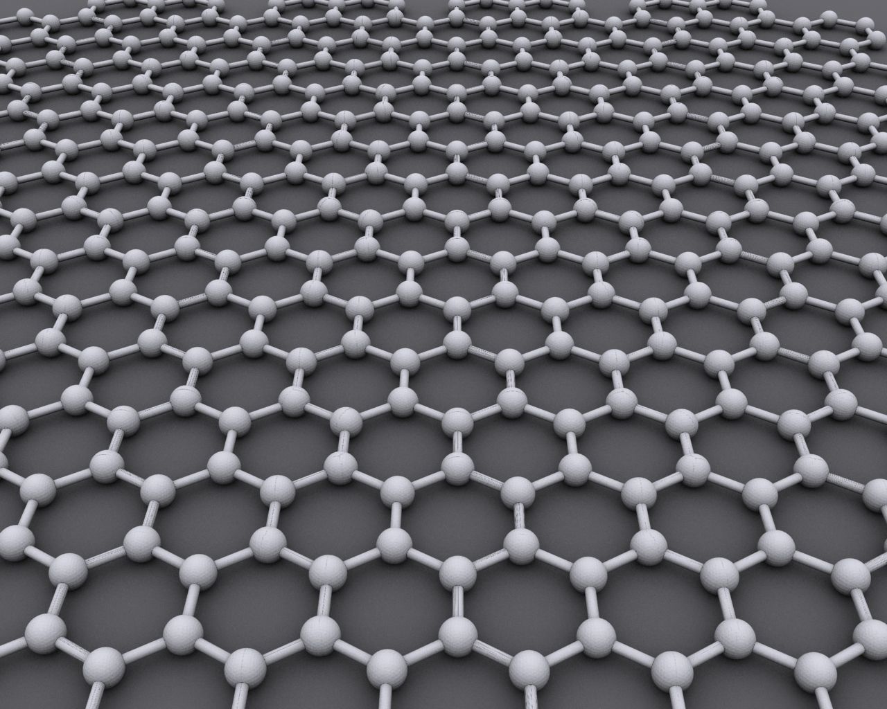
Under de senaste två åren har vi hört väldigt mycket om grafen och dess potential som ersättare till kisel i datorchip. Grafen är en tunn skiva av kol med en atoms tjocklek och dess egenskaper är väldigt lovande. Det återstår bara ett problem, ett lämpligt sätt att tillverka det på.The New Yorker har en ganska lång artikel om grafen och dess upptäckare, Andre Geim, såväl som en av de fysiker som leder en större del av den forskning kring grafen som nu pågår, James Tour. Nedan följer ett kort utdrag ur artikeln som förklarar en del av problemen med grafen."[S]cientists are still trying to devise a cost-effective way to produce graphene at scale. Companies like Samsung use a method pioneered at the University of Texas, in which they heat copper foil to eighteen hundred degrees Fahrenheit in a low vacuum, and introduce methane gas, which causes graphene to "grow" as an atom-thick sheet on both sides of the copper—much as frost crystals "grow" on a windowpane. They then use acids to etch away the copper. The resulting graphene is invisible to the naked eye and too fragile to touch with anything but instruments designed for microelectronics. The process is slow, exacting, and too expensive for all but the largest companies to afford. ... Nearly every scientist I spoke with suggested that graphene lends itself especially well to hype".
newyorker.com
PC,
Övrigt,
Grafen,
38.7°
0
Samuel Paulsson
tis. 16 dec 2014, 09:00
+
Per månad
39 kr
Betala löpande per månad. Ingen bindningstid.
Starta prenumeration
Per år
299 kr
Enklast och billigast, bara 25 kronor i månaden. Betala löpande per år. Ingen bindningstid.
Prova 14 dagar gratis innan du bestämmer dig.
Starta gratis provperiod
Engångsköp
349 kr
Slipp återkommande betalningar, betala ett år i taget. Betala med kort eller Swish.
Köp utan prenumeration